


Printed Circuit Boards are considered the foundation of modern electronic devices. Past PCBs were simpler and limited by processing techniques. But modern printed circuit boards are a bit more complex and advanced.
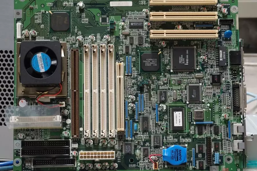
Although PCBs for simple devices are composed of a single layer, sophisticated electronic gadgets such as computer motherboards consist of multiple layers. Printed circuit boards with more than two layers are known as multilayer PCBs.
Please continue reading to learn more about multilayer PCBs, their benefits, disadvantages, manufacturing process, and applications.
What Is Multilayer PCB?
A multilayer PCB is a circuit board of three or more copper foil layers. Single- and double-layer PCBs are combined with a complex printed circuit board.
The lowest number of conductive layers for multilayer PCBs is three, but you can incorporate even a hundred layers based on your needs. Multilayer PCBs are rigid because it is hard to produce flexible multilayer boards.
Most multilayer PCBs have 4 to 8 layers, but devices such as smartphones can incorporate 12 layers. This is because they fit well with the complexity of the application.
Most manufacturers of multilayer PCBs prefer even numbers of layers over an odd number of layers. This is because laminating an odd number can make the circuit board a bit complex and might have issues. Also, the cost is another factor you cannot ignore.
In multilayer printed circuit boards, some layers can be assigned fixed tasks. Layers with fixed tasks as known as planes. You can have ground planes or power planes.
Also, layers in multilayer PCBs are connected in different styles. They can be associated with each other through Buried Via, Blind Via, or Through-hole Via.
Benefits Of Multilayer PCB
Many electronic devices are using multilayer PCBs due to their numerous benefits. Some of the main advantages of multilayer PCBs include:
Small size
One of the main advantages of multilayer PCB is its small size. And even though it is small, it is reliable and very effective.
The older models used 4 to 8 layered PCBs, but modern ones use 12 and more layered PCBs. Thus, modern electronic devices such as microwaves, smartphones, and others are updating their models.
Lightweight
Apart from being small, multilayer PCBs are very light. And this feature can be used in hand-held gadgets such as electronic watches, mobile phones, blood pressure monitors, and others.
High Durability
Another advantage of multilayer PCBs is durability. Since experts design them, the manufacturing process is advanced and precise. Moreover, they are reliable, effective, and durable.
Incredible power in a small package
Due to multilayer printed circuit boards, modern electronic devices are smaller in size. There is also an opportunity to add more electronic elements in a small space.
In addition, the density of elements can be boosted by increasing the number of layers. This is one of the reasons why mobile gadgets are becoming smaller and more powerful over time.
Disadvantages Of Multilayer PCB
Even though multilayer PCBs come with many benefits, there are a few disadvantages. Some of the drawbacks of PCBs include:
High manufacturing costs
The main disadvantage of multilayer PCBs is the cost of manufacturing. Since the manufacturing process is a bit complex, you can expect the costs to be higher than those of standard PCBs.
More manufacturing time
Unlike other types of PCBs, such as single-layer and double-layer PCBs, multilayer printed circuit boards need more manufacturing time. This is because the PCBs require a lengthy process such as lamination, printing, and joining.
Moreover, the manufacturing time depends on the quality and complexity of the gadget. But for a simpler order, it can take a week or more.
Challenging to repair and debug
Another disadvantage of multilayer PCBs is that it is hard to repair or debug compared to simple PCBs that are easy to debug. However, due to this challenge, most companies first design prototypes to eliminate bugs and errors before going to full production.
Professional designers are needed
When it comes to designing a multilayer PCB, the process is a bit challenging. For example, if there is a design problem in the present model, you will be forced to redo the process.
Therefore, a team of professional designers is needed to design multilayer PCBs. Also, if the electronic design is more complex, multiple teams of designers are required.
The Manufacturing Process Of Multilayer PCB
Designing CAD model – the first manufacturing step involves designing the software model of a multilayer printed circuit board. The designing tools used to create PCB layouts include Proteus, Altium, and others.
Since designing multilayer PCBs is a bit complex, professional designers and experts are needed. Once the designs are ready, the next step is to look for a manufacturer.
Finding a PCB manufacturer – there are many multilayer PCB manufacturers you can consider. However, you need to understand that companies offer different prices and quality.
Some essential things you need to check when looking for a PCB manufacturer include Via styles, the maximum number of layers, drill sizes, and layers thickness.
Manufacturing of PCBs – With the completion of PCB design and having a manufacturer, the next step is manufacturing the boards. It has several processes in the manufacturing, such as drilling, silkscreen, etching, CNC milling and so on.
Here, prepreg and core materials are joined together and are exposed to high pressure and temperature. This is to remove any trapped air between different layers.
PCBs are manufactured from different materials. You can decide to have your PCBs made from epoxy glass, exotic ceramic, Teflon, and other materials.
Multilayer PCB testing – the manufacturing of PCB is completed; it needs to be tested. This is done to check whether there are errors or if it is manufactured as requested.
Applications Of Multilayer PCBs
Multilayer PCBs have found themselves everywhere. You will find the circuit boards in mobile phones, computers, home automated systems, shaving machines, radar systems, broadcasting systems, signal transmission systems, and medical devices.
Other applications of multilayer PCBs are atomic accelerators, weather analysis, GPS technology, space probe equipment, data storage, file servers, fiber optic receptors, and others.
Bottom-Line
With the progression of technology, the uses of multilayer PCBs are expected to grow. Hence, your company needs to invest in the latest trends and focus more on multilayer PCBs.
With the above information, you can now decide whether it is worth using multilayer printed circuit boards. However, make sure you engage professionals when designing and manufacturing multilayer PCBs.


![Fan Expo Chicago [Convention], Donald E. Stephens Convention Center, 16 Aug What You Need to Know](https://www.thefreemanonline.org/wp-content/uploads/2024/09/Fan-Expo-Chicago-Convention-Donald-E.-Stephens-Convention-Center-16-Aug-What-You-Need-to-Know-74x55.jpg)
![Error [err_http_headers_sent] Cannot Set Headers After They Are Sent to the Client How to Fix](https://www.thefreemanonline.org/wp-content/uploads/2024/09/Error-err_http_headers_sent-Cannot-Set-Headers-After-They-Are-Sent-to-the-Client-How-to-Fix--74x55.jpg)
